Wafer Backgrind
Wafer Backgrind is the process of grinding the
backside of the wafer to the correct wafer thickness prior to
assembly. It is also referred to as
'wafer thinning.' Wafer backgrinding has not always been necessary,
but the drive to make packages thinner and thinner has made it
indispensable.
Most package types in the
semiconductor industry today would require a wafer thickness ranging
from 8 mils to 20 mils.
Wafers
normally undergo a cleaning and surface lamination process prior to the
actual backgrinding process. Surface lamination involves the application of a
protective
tape over the surface of the wafer to protect it from mechanical damage
and contamination during backgrinding.
The
surface-laminated wafers are then loaded into
cassettes that will go
into the cassette holder of the backgrinding machine.
The machine picks up the wafer from its backside (untaped side)
with a robotic arm, which positions the wafer for backgrinding.
The backgrinding process is automatically accomplished by a
grinding
wheel, following a precise set of parameters to ensure proper backgrinding.
To remove
debris from the wafer while backgrinding, the wafer is usually
washed
continuously with D/I water while undergoing backgrinding.
Once the wafer has been background, the wafer is returned to the
cassette, and the cycle is repeated for the next wafer.
Parameters
set for backgrinding include spindle speed, spindle coolant water
temperature and flow rate, D/I water temperature, initial and final
wafer thickness, and feed speeds.
See also:
Backgrind Failure Mechanisms
|
 |
|
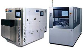
Fig. 1.
Photos of Backgrind Systems |
Front-End Assembly
Links:
Wafer Backgrind;
Die Preparation;
Die Attach;
Wirebonding;
Die Overcoat
Back-End Assembly
Links:
Molding;
Sealing;
Marking;
DTFS;
Leadfinish
See Also:
Backgrind Failure Mechanisms;
IC
Manufacturing; Assembly Equipment
HOME
Copyright
©
2001-2006
www.EESemi.com.
All Rights Reserved.