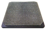
The
Ceramic
Column
Grid Array,
or CCGA,
is
a square-shaped or rectangular ceramic package that uses solder columns for
external electrical connection instead of leads or solder balls. These solder
columns are arranged in a grid or
array at the bottom of the ceramic package body, hence the name 'ceramic
column grid array'. The
CCGA is basically just a CBGA package that has
solder columns instead of solder balls.
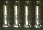
The main advantage of CCGA over CBGA is
the higher reliability of the solder columns compared to solder balls.
The columns provide a higher package stand-off and structural
flexibility, allowing the CCGA to adapt to CTE mismatches with the PCB
more easily than CBGA's.
The CCGA package is designed for high
I/O applications, with column counts typically ranging from 191 to 2577.
Column
pitch
(distance between
solder columns) values typically used by the CCGA package are 1.0 mm and 1.27 mm. Typical CCGA body sizes range from
14 mm square to 52.5 mm square. The height of the solder column from the
ceramic body of the CCGA is typically either 1.27 mm or 2.2 mm.
Table 1.
Properties of Some CCGA's
|
No. of
Columns |
Body
Size |
Package
Thickness |
Column Pitch |
|
376 |
27.94 mm x
27.94
mm |
2.79 mm |
1.27 mm |
|
376 |
27.94 mm x
27.94
mm |
2.79 mm |
1.27 mm |
|
624 |
32.5 mm x
32.5
mm |
2.5 mm |
1.27 mm |
|
1152 |
35 mm x 35
mm |
3 mm |
1.0 mm |
|
1272 |
37.5 mm x
37.5
mm |
3 mm |
1.0 mm |