EESemi.com FAQ
- questions most frequently asked by visitors of www.EESemi.com
Distinguishing EOS from ESD
How can one
distinguish an EOS damage from an ESD damage?
In many
cases, it is not difficult to distinguish between an electrical
overstress (EOS) and an electrostatic discharge (ESD) damage. For
instance, we're all
quite comfortable assigning gross failure attributes such as extensive
metal line burn-out and migration
to EOS. When we see that the package is discolored and
carbonized, as well as difficult to decapsulate,
then we also know that it was exposed to a large amount of heat
characteristic of an EOS rather than an ESD event.
On the
other hand, subtle defects that usually require high electric fields or
voltages to arise such as dielectric or oxide punchthroughs are often
attributed to ESD. This is especially true if the affected area is
close to an external pin, and historical and technical data show that
the area is indeed vulnerable to an ESD event. One example is a
capacitor connected directly to an unprotected external pin of an
ESD-sensitive device.
Still, there
will always be many cases wherein the failure attributes exhibited by a
device are definitely due to an EOS or ESD event, yet not absolutely
traceable to either one of them. An example of this is mild metal
burn-out or migration, which can be caused by either a weak electrical
overstress or a strong ESD event. Fused resistors are also known
to be caused either by EOS or ESD. 'Gray area' cases such as these
are the ones that are difficult to trace to the actual root cause.
In such
cases, the engineer analyzing the failures has no choice but to
complement the results of the failure analysis techniques with a
thorough investigation of the circumstances surrounding the affected
units, from their design and qualification to their actual use in the
field. This would include analyzing qualification and reliability
data, lot histories, equipment
set-ups, and even operator assignments, so that any discernible pattern
exhibited by the affected lots can be given greater focus.
Unfortunately, such an endeavor is complicated by the fact that
attributes can change over time and as the units undergo processing.
For instance, a gross EOS failure attribute may have originated from a
subtle ESD damage that was just aggravated into a full-blown EOS damage
during electrical testing.
Simulation is a good method for confirming a cause, but it is only
effective if the appropriate simulation conditions can be defined and
executed with reasonable control, and if the failure attributes are
exactly replicated by the simulation performed. Being able to
trace the discharge path of an ESD event or the damage path of an EOS
event based on failure attributes exhibited by the samples also adds
value to root cause analysis, but it is not
applicable to all cases.
|
|
|
 |
|
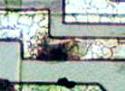
Figure 1. Gross
metal burn-out is often due to EOS.
|
|
Only by
gathering as much information as possible and comprehending them
holistically can a sound conclusion on
whether the failure cause is EOS or ESD
be reached. Nonetheless, an
engineer must understand that he or she has limited powers, and can not
be expected to arrive at the exact failure root cause 100% of the time.
Even when the analysis boils down to simply choosing between ESD or EOS
as the culprit, attributes can be too vague to reveal the true identity
of their source.
Without
tell-tale signs from data analysis, or successful simulation or discharge/damage path tracking results, one has
to resort to a 'shot gun' approach wherein all possible sources of EOS
and ESD on the line are identified systematically and eliminated accordingly.
Continuous improvement of the line is a 'must' in such a
case, until the problem disappears altogether.
See Also:
Electrical Testing;
Electrical Overstress
Back to the FAQ Page...
HOME
Copyright
©
2006
EESemi.com.
All Rights Reserved.