Marking
Marking is the process of putting
identification, traceability, and distinguishing
marks on the package of an IC.
The device name, company logo, date code, and lot id are examples
of information commonly marked on the IC's package. Some marks are
put on the package during Assembly and some marks are put on the package
during Test.
There are two common
marking processes, namely,
ink marking and
laser marking.
The most common ink marking process for semiconductor products is
pad printing. Pad printing consists of transferring an
ink pattern from the
plate, which is a flat block with pattern depressions that are filled
with ink, to the package, using a
silicone rubber stamp pad. Silicone rubber repels ink, making the transfer of the ink
pattern clean and efficient. It
is also resilient and elastic, making it possible to print even on
uneven surfaces.
|
 |
|
Fig. 1.
Photos of Silicone Rubber Pads used for Ink Marking |
Simply put, the pad printing process
can be broken down into the following steps: a) the stamp pad passes over the surface of the ink; b) the
surface ink sticks to the pad; c) the
pad is applied to the surface for marking; and d) the ink sticks to the
marking surface as the pad lifts. Ink
marking is usually punctuated by
ink curing.
Aside from mark quality,
mark permanence is a critical aspect of IC package marking.
Mark permanence failures can be due to a lot of things such as
use of inappropriate ink, use of improperly prepared ink, inadequate ink
curing, and marking surface contamination.
Good wetting of the ink on the marking surface is necessary for
good marking. For wetting to occur, the surface tension of the ink must
be less than the surface tension of the marking surface.
Thus, a careful review and interpretation of the surface tension
data of the ink to be used and those of the intended marking surface is
needed to ensure good ink marking.
Laser
marking, as
the name implies,
refers to the process of
engraving marks on the marking surface using a
laser beam. There are many
types of lasers, but the ones used or in use in the semiconductor
industry include the CO2 laser, the YAG laser, and diode lasers.
In the semiconductor industry, lasers can also be used in
micromachining, surface processing, trimming, welding, and cutting.
|
 |
|
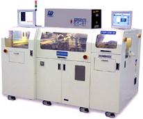
Figure 2.
Example of a Laser Marker |
Common
marking
failure
attributes
include the following: 1) missing
mark; 2) missing character; 3) misoriented mark; 4)
wrong
mark format; 5) misplaced mark; 6) mark
permanency failure; and 7)
inadequate
mark contrast. For more
details on marking failure attributes,
see also:
Marking Failures.
Front-End Assembly
Links:
Wafer Backgrind;
Die Preparation;
Die Attach;
Wirebonding;
Die Overcoat
Back-End Assembly
Links:
Molding;
Sealing;
Marking;
DTFS;
Leadfinish
Test Links:
Electrical
Test; Burn-in;
Tape and Reel; Dry Packing;
Boxing and Labeling
See Also:
Laser Marking; Pad Printing Inks;
IC
Manufacturing; Assembly Equipment
HOME
Copyright
©
2001-2006
www.EESemi.com.
All Rights Reserved.

