The p-n
Junction
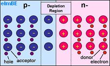
The
p-n junction is the most basic building block of semiconductor
electronics.
It consists of a p-type material in perfect contact with an
n-type material.
The area within the vicinity of the junction is known as the
depletion region, because it is depleted of
mobile carriers (electrons
and holes).
This is because the electrons from the n-type material have
crossed the junction and
diffused into the other side (p-type), recombining with holes in that side.
On the other hand, the holes from the p-type material have
diffused to the n-type material, recombining with electrons.
Because of this diffusion process, holes
not covered by electrons are left in the n-type material, while
electrons not covered by holes are left in the p-type material.
Known
as
uncovered charges, these result in an over-all negative charge in the
p-type material and an over-all positive charge in the n-type material.
This
separation of
charges
develops a
potential across the depletion region,
preventing further diffusion of carriers across the junction.
This potential, known as the
potential
barrier,
is about
0.6- 0.7V
in a typical silicon p-n junction.
|
 |
|
Figure 1. The p-n junction. Note the depletion reqion around
the junction where only immobile uncovered charges (ions) exist |
See Also:
What is a Semiconductor?; Diode; Bipolar
Transistor;
MOSFET;
JFET;
IC Manufacturing
HOME
Copyright
©
2001-2006
www.EESemi.com.
All Rights Reserved.