Physical
Vapor Deposition (PVD) by Sputtering
Physical Vapor
Deposition (PVD) is a process by which a thin film of material is deposited
on a substrate according to the following sequence of steps: 1)
the material to be deposited is converted into vapor by physical means; 2)
the vapor is transported across a region of low pressure from its source
to the substrate; and 3) the vapor undergoes condensation on the
substrate to form the thin film. In VLSI fabrication, the most
widely-used method of accomplishing PVD of thin films is by sputtering.
Sputtering is a mechanism by which atoms are dislodged from the
surface of a material as a result of collision with high-energy particles.
Thus,
PVD by Sputtering is a term used to refer to a physical
vapor deposition (PVD) technique wherein atoms or molecules are ejected from a target
material by high-energy particle bombardment so that the ejected atoms or
molecules can condense on a substrate as a thin film.
Sputtering has become one of the most widely used techniques for
depositing various metallic films on wafers, including aluminum, aluminum
alloys, platinum, gold, TiW, and tungsten.
Sputtering as a deposition technique may be described as a
sequence of these steps: 1) ions are generated and directed at
a target material; 2) the ions sputter atoms from the target; 3) the
sputtered atoms get transported to the substrate through a region of
reduced pressure; and 4) the sputtered atoms condense on the substrate, forming a thin film.
Sputtering
offers the following advantages over other PVD methods used in VLSI
fabrication:
1)
Sputtering can be achieved from large-size targets, simplifying the
deposition of thins with unifrom thickness over large wafers;
2)
Film thickness is easily controlled by fixing the
operating parameters and simply adjusting the deposition time;
3) Control
of the alloy composition, as well as other film properties such as step
coverage and grain structure, is more easily accomplished than by
deposition through evaporation;
4)
Sputter-cleaning of the substrate in vacuum prior to film deposition can
be done;
5)
Device damage from X-rays generated by electron beam evaporation is
avoided.
Sputtering,
however, has the following disadvantages too:
1)
High capital expenses are required;
2)
The rates of deposition of some materials (such as SiO2) are relatively
low;
3)
Some materials such as organic solids are easily degraded by ionic
bombardment;
4)
Sputtering has a greater tendency to introduce impurities in the substrate
than deposition by evaporation because the former operates under a lesser
vacuum range than the latter.
 |
|
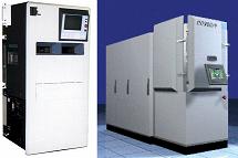
Figure 1.
Examples of Sputter Systems |
The
high-energy particles used in sputter-deposition are generated by glow
discharges. A glow discharge is a self-sustaining type of plasma created
by applying an RF field to a pressurized gas like argon, creating free
electrons within the discharge region. A complete theory on how
sputtering occurs has not yet been established due to the complexity of
interactions involved, but experts in the field state that sputtering is
comparable to billiard ball kinetics in three dimensions.
Sputtering yield, or the
number of atoms ejected per incident ion, is an important factor in
sputter deposition processes, since it affects the sputter deposition
rate. Sputtering yield primarily depends on three major factors:
1) target material; 2) mass of the bombarding particles; and 3) energy
of bombarding particles. In the energy range where sputtering occurs (10
to 5000 eV), the sputtering yield increases with particle mass and
energy.
See Also:
Polysilicon;
Dielectric;
Thin
Films;
Metallization;
Glassivation; PVD
by Evaporation; CVD
HOME
Copyright
© 2001-2004
www.EESemi.com.
All Rights Reserved.